In a single isolated atom, electrons occupy sharply defined energy levels. Bring a large number of atoms together into a crystal, close enough that outer orbitals overlap, and each level broadens into a closely spaced cluster of levels called an energy band. The highest band that contains electrons at absolute zero is the valence band; the band above it, into which an electron must be rais
Semiconductor Electronics
Class 1219 previous-year questions from this chapter every option and the correct answer, free · where the marks are
1. Energy bands, intrinsic and extrinsic semiconductors
Exam focus: Doping never leaves a semiconductor charged — an n-type material has extra free electrons as majority carriers, but the donor ion left behind balances the charge exactly, so the material as a whole stays electrically neutral.
Semiconductor Electronics: Energy Bands, Intrinsic and Extrinsic Semiconductors
NCERT Wallah
Full-chapter one-shot; covers energy bands, intrinsic and extrinsic semiconductors, plus later topics like p-n junction diodes not part of this named subtopic — used because no single dedicated video covers all three together.
PhysicsNEET 2021show ▾The electron concentration in an n-type semiconductor is the same as the hole concentration in a p-type semiconductor. An external electric field is applied across each of them. Compare the currents in them.
- A.Current in n-type = current in p-type
- B.Current in p-type > current in n-type
- C.Current in n-type > current in p-type✓
- D.No current will flow in p-type; current will only flow in n-type
The worked solution is part of a paid pack.
PhysicsNEET 2020show ▾The solids which have a negative temperature coefficient of resistance are:
- A.Metals
- B.Insulators only
- C.Semiconductors only
- D.Insulators and semiconductors✓
The worked solution is part of a paid pack.
PhysicsNEET 2020show ▾For transistor action, which of the following statements is correct?
- A.Base, emitter and collector regions should have the same doping concentrations
- B.Base, emitter and collector regions should have the same size
- C.Both the emitter junction and the collector junction are forward biased
- D.The base region must be very thin and lightly doped✓
The worked solution is part of a paid pack.
PhysicsNEET 2019show ▾For a p-type semiconductor, which of the following statements is true?
- A.Electrons are the majority carriers and trivalent atoms are the dopants
- B.Holes are the majority carriers and trivalent atoms are the dopants✓
- C.Holes are the majority carriers and pentavalent atoms are the dopants
- D.Electrons are the majority carriers and pentavalent atoms are the dopants
The worked solution is part of a paid pack.
2. p-n junction diode, rectifiers, Zener diode
Exam focus: A Zener diode is the one diode deliberately operated in reverse breakdown, using its near-constant voltage there for regulation — every ordinary diode is designed to avoid that same region. A full-wave rectifier conducts on both halves of the input cycle; a half-wave rectifier, only one.
p-n Junction Diode and Rectifiers (Class 12)
Aakash NEET
Covers p-n junction formation, the depletion region, forward/reverse bias, and half-wave and full-wave rectifier circuits in a focused, well-scoped lecture. It does not appear to cover Zener diode voltage regulation, so that part of the subtopic is likely missing here.
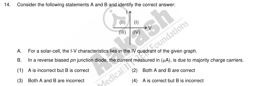
PhysicsNEET 2024show ▾Consider the following statements A and B and identify the correct answer (refer to the given – graph):
A. For a solar cell, the – characteristic lies in the IV quadrant of the given graph.
B. In a reverse-biased p-n junction diode, the current measured (in A) is due to majority charge carriers.
- A.A is incorrect but B is correct
- B.Both A and B are correct
- C.Both A and B are incorrect
- D.A is correct but B is incorrect✓
Solution
A solar cell's – curve lies in the fourth quadrant (it delivers power, so and have opposite signs) — A is correct. Reverse current in a p-n junction is carried by minority carriers — B is incorrect.
Open this question on its own page →
Save for spaced revision (free account)PhysicsNEET 2023show ▾Given below are two statements:
Statement I: Photovoltaic devices can convert optical radiation into electricity.
Statement II: A Zener diode is designed to operate under reverse bias in the breakdown region.
In the light of the above statements, choose the most appropriate answer from the options given below:
- A.Both Statement I and Statement II are correct✓
- B.Both Statement I and Statement II are incorrect
- C.Statement I is correct but Statement II is incorrect
- D.Statement I is incorrect but Statement II is correct
The worked solution is part of a paid pack.
PhysicsNEET 2023show ▾A full-wave rectifier circuit consists of two p-n junction diodes, a centre-tapped transformer, a capacitor and a load resistance. Which of these components removes the AC ripple from the rectified output?
- A.A centre-tapped transformer
- B.p-n junction diodes
- C.Capacitor✓
- D.Load resistance
The worked solution is part of a paid pack.
PhysicsNEET 2022show ▾In half-wave rectification, if the input frequency is 60 Hz, then the output frequency would be:
- A.120 Hz
- B.Zero
- C.30 Hz
- D.60 Hz✓
The worked solution is part of a paid pack.
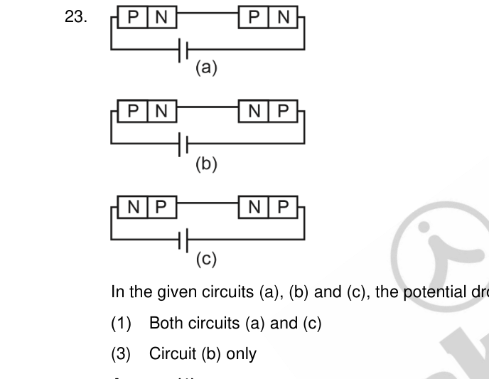
PhysicsNEET 2022show ▾In the given circuits (a), (b) and (c), the potential drop across the two p-n junctions are equal in:
- A.Both circuits (a) and (c)✓
- B.Circuit (a) only
- C.Circuit (b) only
- D.Circuit (c) only
The worked solution is part of a paid pack.
PhysicsNEET 2021show ▾Consider the following statements (A) and (B) and identify the correct answer.
(A) A Zener diode is connected in reverse bias when used as a voltage regulator.
(B) The potential barrier of a p-n junction lies between 0.1 V and 0.3 V.
- A.(A) and (B) both are correct
- B.(A) and (B) both are incorrect
- C.(A) is correct and (B) is incorrect✓
- D.(A) is incorrect but (B) is correct
The worked solution is part of a paid pack.
PhysicsNEET 2020show ▾The increase in the width of the depletion region in a p-n junction diode is due to:
- A.Forward bias only
- B.Reverse bias only✓
- C.Both forward bias and reverse bias
- D.Increase in forward current
The worked solution is part of a paid pack.
3. Logic gates
Exam focus: NAND and NOR are each called a universal gate because either one alone, used repeatedly, can build every other basic gate — AND, OR and NOT included — which is why real circuits are so often built almost entirely from just one of them.
Digital Electronics and Logic Gates (NCERT)
NCERT Wallah
Directly covers AND/OR/NOT/NAND/NOR gates and truth tables as the 'Digital Electronics' section of the NCERT semiconductor chapter — a clean, focused match for this subtopic.
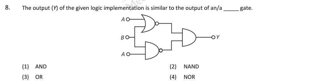
PhysicsNEET 2025show ▾The output () of the given logic implementation is similar to the output of a/an _____ gate.
- A.AND
- B.NAND
- C.OR
- D.NOR✓
Solution
The top gate is a NOR: . The bottom gate is a NAND: . Their AND gives , which is exactly — a NOR gate.
Open this question on its own page →
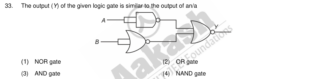
Save for spaced revision (free account)PhysicsNEET 2024show ▾The output () of the given logic gate circuit is similar to the output of a/an:
- A.NOR gate
- B.OR gate
- C.AND gate✓
- D.NAND gate
Solution
The upper gate has both inputs tied to A, so it outputs ; the lower NOR with both inputs B outputs . The final NOR gives — an AND gate.
Open this question on its own page →
Save for spaced revision (free account)PhysicsNEET 2024show ▾A logic circuit provides the output as per the following truth table:
A B Y 0 0 1 0 1 0 1 0 1 1 1 0
The expression for the output is:
- A.
- B.✓
- C.
- D.
Solution
The output is 1 exactly when , regardless of — the table is that of .
Open this question on its own page →
Save for spaced revision (free account)PhysicsNEET 2023show ▾For the logic circuit shown, the truth table is:
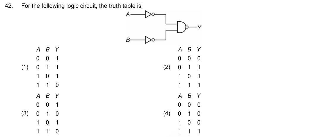
- A.A B Y: 0 0 1 · 0 1 1 · 1 0 1 · 1 1 0
- B.A B Y: 0 0 0 · 0 1 1 · 1 0 1 · 1 1 1✓
- C.A B Y: 0 0 1 · 0 1 0 · 1 0 1 · 1 1 0
- D.A B Y: 0 0 0 · 0 1 0 · 1 0 0 · 1 1 1
The worked solution is part of a paid pack.
PhysicsNEET 2022show ▾The truth table for the given logic circuit is:
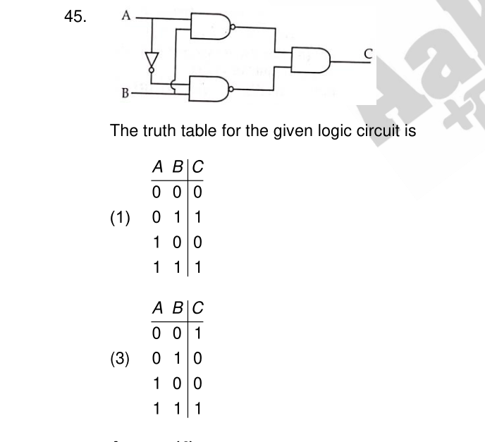
- A.A B C: 0 0 0 · 0 1 1 · 1 0 0 · 1 1 1
- B.A B C: 0 0 0 · 0 1 1 · 1 0 1 · 1 1 0
- C.A B C: 0 0 1 · 0 1 0 · 1 0 0 · 1 1 1
- D.A B C: 0 0 1 · 0 1 0 · 1 0 1 · 1 1 0✓
The worked solution is part of a paid pack.
PhysicsNEET 2021show ▾For the given circuit, the input digital signals are applied at the terminals A, B and C. What would be the output at the terminal y?
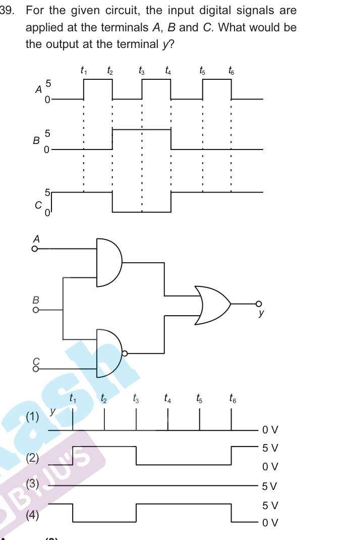
- A.Waveform (1)
- B.Waveform (2)
- C.Waveform (3)✓
- D.Waveform (4)
The worked solution is part of a paid pack.
PhysicsNEET 2020show ▾In the logic circuit shown, inputs A and B are each first passed through a NOT gate, and the two outputs are then fed into a NOR gate to give output Y. The truth table for Y is:
- A.A B Y: 0 0 0 · 0 1 0 · 1 0 0 · 1 1 1✓
- B.A B Y: 0 0 0 · 0 1 1 · 1 0 1 · 1 1 1
- C.A B Y: 0 0 1 · 0 1 1 · 1 0 1 · 1 1 0
- D.A B Y: 0 0 1 · 0 1 0 · 1 0 0 · 1 1 0
The worked solution is part of a paid pack.
PhysicsNEET 2019show ▾In the circuit shown, inputs A and B each control a diode into a common node, which is tied through a resistor to V and also drives an LED (Y) to ground: the node — and the LED, which lights when the node is LOW — is pulled LOW whenever at least one of A, B is LOW (0), and goes HIGH (LED off) only when both A and B are HIGH (1). This gives the truth table A,B Y: 0,0 1; 0,1 1; 1,0 1; 1,1 0. The correct Boolean operation represented by this circuit is:
- A.AND
- B.OR
- C.NAND✓
- D.NOR
The worked solution is part of a paid pack.